

Product Name: Ultra-High Purity Semiconductor Ceramic Sleeve
Product Material: High-Purity Alumina ($Al_2O_3 \ge 99.8\%$), Sintered Silicon Carbide (SSiC), Aluminum Nitride (AlN), or High-Purity Quartz.
Material Characteristics: Ultra-high purity (minimal metallic impurities), Excellent resistance to plasma erosion (fluorine/chlorine-based), Exceptional dielectric strength, Vacuum-tight with zero porosity, Low coefficient of thermal expansion, High thermal conductivity (for AlN/SiC grades), Minimal outgassing.
Application Fields: Plasma etch chamber insulators, Wafer lift pin sleeves, Gas distribution system bushings, Ion implantation beamline liners, Thermal couple protection in diffusion furnaces, MOCVD reactor components, Electrostatic chuck (ESC) peripheral sleeves.
Application Industries: Broad Semiconductor (Front-end wafer fabrication), Electronic Engineering (Power device manufacturing), New Energy (Advanced solar cell processing), Aerospace (High-precision sensors).
Processing Difficulties: Achieving stringent surface cleanliness (Class 10/100 cleanroom standards), Controlling metallic ion contamination (e.g., Na, K, Fe) to ppb levels, Managing micron-level geometric tolerances on thin-walled components, Achieving atomic-level surface smoothness to prevent particle generation during plasma exposure.
Processing Flow: Ultra-pure powder preparation → Clean-room Isostatic Pressing → Precision Green Machining → High-purity sintering (Atmosphere controlled) → Diamond precision grinding → Chemical etching (to remove surface damage layers) → Ultrasonic deionized water cleaning → Class 100 cleanroom inspection & vacuum packaging.
Delivery Period: Standard specifications: 25-40 days,
Our ultra-high purity ceramic sleeve, crafted from alumina ceramic parts and custom materials, delivers exceptional chemical resistance and thermal stability, ensuring contamination-free semiconductor manufacturing.

Functionally Specialized for Semiconductor Fabrication Reliability
This ultra-high purity ceramic sleeve serves as a critical component within semiconductor wafer fabrication equipment, designed specifically for contamination control and long-term durability. Targeted at semiconductor manufacturers and equipment engineers, it provides a stable interface to plasma etching and high-temperature processes. Manufactured using advanced alumina ceramic machining techniques, the sleeve ensures vacuum-tight integrity and minimal particulate generation, addressing stringent fabrication cleanliness requirements essential for sustaining production yields in highly sensitive process chambers.
Precision Manufacturing and Measurable Technical Excellence
Engineered with over 99.8% pure alumina ceramic, as well as available variants of sintered silicon carbide and aluminum nitride, the sleeve offers outstanding resistance to corrosive fluorine and chlorine plasmas. Its non-porous, vacuum-tight structure prevents outgassing while high thermal conductivity grades optimize temperature management in demanding environments. Strict dimensional tolerances and smooth atomic-level finishes are achieved through cleanroom isostatic pressing, diamond grinding, and chemical etching, ensuring each part meets rigorous cleanliness standards and long maintenance intervals required by the semiconductor industry’s process tool specifications.
Enhancing Semiconductor Process Chamber Performance Across Applications
The sleeve’s chemical inertness and thermal stability position it as a versatile solution for multiple semiconductor equipment components, including plasma etch chamber insulators, gas distribution bushings, and ion implantation liners. Integrating seamlessly into semiconductor front-end fabrication tools, these components protect sensitive wafer environments from contamination and mechanical wear, thereby extending tool life and optimizing uptime. This product supports advanced node process requirements where metal impurity control and zero particle generation directly impact process yield and overall operational efficiency.
Designed specifically for the rigorous environment of wafer fabrication, our Semiconductor Ceramic Sleeves provide the ultimate barrier against contamination and thermal stress. Whether used in plasma etching or high-temperature diffusion, these sleeves ensure that critical process parameters are maintained without shedding particles or leaching trace metals. By utilizing specialized high-density sintering techniques, we provide components that resist the aggressive chemical attacks of fluorine and chlorine gases, significantly extending the maintenance cycles of the process chamber and ensuring high yields for sensitive node technologies.
Key Features:
Contamination Control: Manufactured with high-purity materials to ensure zero trace-metal interference with silicon wafers.
Plasma Erosion Resistance: Optimized microstructure provides superior longevity in aggressive RF plasma environments.
Vacuum Stability: High-density, non-porous body ensures zero outgassing and maintains hermetic chamber integrity.
Thermal Management: Available in high-thermal-conductivity grades (AlN/SiC) for precise temperature control during processing.
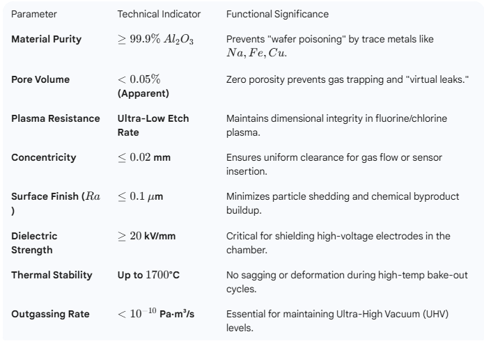
Our Market Advantages
What high-purity ceramic materials are used for your semiconductor ceramic sleeves?
We manufacture our sleeves using ultra-high purity materials such as alumina ceramic ($Al_2O_3 \ge 99.8\%$), sintered silicon carbide (SSiC), aluminum nitride (AlN), and high-purity quartz. These materials offer excellent chemical resistance, thermal stability, and maintain zero particle generation during semiconductor manufacturing.
Can you customize alumina ceramic sleeves for specific wafer fabrication requirements?
Yes, we offer custom alumina ceramic sleeves tailored to your specifications. Our precision machining and strict dimensional tolerances ensure the sleeves meet demanding semiconductor process conditions, including contamination control and thermal management requirements.
How do you ensure contamination control during the ceramic sleeve manufacturing process?
We produce all sleeves under Class 10/100 cleanroom standards, using ultra-pure powder and atmosphere-controlled sintering to maintain metallic impurities at ppb levels. This process ensures that our ceramic parts have zero porosity and are vacuum-tight with no outgassing, critical for contamination-free semiconductor fabrication.
What is the typical delivery time and logistics for your industrial ceramic solutions?
Standard specifications for our Ultra-High Purity Semiconductor Ceramic Sleeves are delivered within 25-40 days. We coordinate logistics to ensure timely delivery, supporting your production schedule with reliable supply and consistent product quality.


